This case study demonstrates how machine learning can be applied to model and forecast process-level economics in semiconductor manufacturing. A simplified CMOS wafer fabrication line consisting of ten distinct steps was used to simulate time and cost parameters, forming the basis for synthetic training data. A neural network was developed to predict total wafer processing cost based on these stepwise inputs.
Using 5000 training samples and ±5% random noise, a 64-64-1 neural network architecture achieved an R² of 0.8671 and a mean absolute error (MAE) of $85.69 on unseen test data. These results are strong given that the process cost values span a range from approximately $2200 to $4200.
The model supports rapid economic inference and enables simulation of what-if scenarios across fabrication conditions. More broadly, this approach illustrates how Business ML (BML) can be applied to any structured process where time and cost parameters are distributed across sequential operations. The methodology generalizes beyond semiconductors and can be adapted to manufacturing systems, chemical processing, pharmaceutical production, and other domains where cost forecasting plays a critical decision-making role.

Introduction
Business decisions in manufacturing often depend on understanding how time, resources, and process complexity translate into economic outcomes. While many industries rely on spreadsheets or rule-of-thumb estimates to forecast costs, these methods are often slow, rigid, and poorly suited to managing complex, multistep operations. This is where Business ML (BML), the application of machine learning to economic inference, offers a compelling alternative.
This case study applies a Business ML approach to a simplified CMOS (complementary metal-oxide-semiconductor) wafer fabrication process. The semiconductor industry is well suited for cost modeling because of its highly structured process flows, detailed time and equipment usage data, and the economic sensitivity of each fabrication step. By simulating time and cost inputs across ten key process stages, a neural network model was trained to predict total wafer processing cost with strong accuracy and generalization.
Unlike traditional process optimization models that focus on physics or yield, the objective here is economic. The aim is to estimate the total cost per wafer given variations in time and cost rates across steps such as oxidation, photolithography, etching, and deposition. This reframes machine learning as a tool for business reasoning rather than scientific analysis.
The goal of this article is to demonstrate how Business ML can provide fast, scenario-ready predictions in structured process environments. It offers a way for engineers, planners, and decision-makers to simulate cost impacts without manually recalculating or maintaining large spreadsheet models. The CMOS process provides a focused example, but the methodology can be extended to any industry where costs accumulate through a sequence of measurable operations.
The CMOS Cost Modeling Problem
Wafer fabrication in CMOS semiconductor manufacturing is a highly structured, stepwise process involving repeated cycles of deposition, patterning, etching, and inspection. Each step contributes incrementally to the final product and to the total manufacturing cost. For modeling purposes, this study uses a simplified version of the CMOS flow that includes ten representative steps: Test & Inspection, Oxidation, Photolithography, Etching, Ion Implantation, Deposition, Chemical Mechanical Planarization (CMP), Annealing, Metallization, and Final Test.
Each step is modeled using two parameters:
- ti, the time required to perform the step, in minutes
- ci, the effective cost per minute associated with the step, which may include equipment usage, labor, power, and materials
The total wafer processing cost is modeled using the following structure:
Process Cost = c_rm + Σ(ki × ti × ci)
for i = 0 to 9
where:
- c_rm is the raw material cost, representing the wafer or substrate being processed
- ti and ci are the time and cost for each of the ten fabrication steps
- ki is an optional step weight or scaling factor, set to 1.0 in this study
This formulation mirrors the approach used in other Business ML applications, such as pharmaceutical cost modeling, where c_rm represents the cost of purchased raw materials and the summation captures stepwise transformation and processing costs.
Because detailed cost data for semiconductor process steps is often proprietary, this study relies on synthetic data generation. Reasonable upper and lower bounds for time and cost were defined for each step based on open-source literature, technical papers, and process engineering judgment. Random values were sampled within these bounds to reflect natural process variation. An additional ±5% random noise term was applied to simulate real-world uncertainty.
This modeling framework is well suited for Business ML. The process is modular, the economic output is driven by well-understood operations, and the structure aligns with common business scenarios where costs are accumulated through a sequence of steps. This enables the trained model to act as a surrogate for estimating cost outcomes without requiring manual spreadsheet calculations or custom economic models.
Model Design and Training
The goal of this model is to predict the total processing cost of a CMOS wafer based on time and cost inputs from each fabrication step. To focus specifically on operational drivers, the model is trained only on the variable portion of the cost:
Process Cost = Σ(ki × ti × ci)
for i = 0 to 9
The fixed raw material cost, denoted as c_rm, is deliberately excluded from the machine learning target. While c_rm contributes to the full wafer cost, it does not depend on process dynamics, and its exclusion allows the model to learn the economic impact of process-specific variation alone.
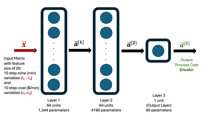
A feedforward neural network was selected for this task, using 20 input features (Table 1):
- Ten step durations (ti) and ten corresponding step costs (ci)
- Each input was standardized using scikit-learn’s StandardScaler
- The output (process cost) was also standardized before training and later inverse-transformed for evaluation
Table 1. Summary of CMOS process step descriptions, time (ti) ranges, and cost rate (ci) ranges used for synthetic data generation
| Step | Description | Time – ti (min) | Cost Rate – ci ($/min) |
| S0 | Test & Inspection – Initial | 10 – 15 | 3.0 – 6.0 |
| S1 | Oxidation | 90 – 150 | 4.0 – 7.0 |
| S2 | Photolithography | 25 – 45 | 12.0 – 20.0 |
| S3 | Etching | 15 – 30 | 8.0 – 14.0 |
| SS4 | Ion Implantation | 10 – 20 | 10.0 – 16.0 |
| S5 | Deposition | 30 – 60 | 6.0 – 10.0 |
| S6 | CMP | 20 – 40 | 5.0 – 9.0 |
| S7 | Annealing | 45 – 90 | 5.0 – 8.0 |
| S8 | Metallization | 30 – 60 | 7.0 – 12.0 |
| S9 | Test & Inspection – Final | 10 – 25 | 3.0 – 6.0 |
The final model architecture consists of:
- Two hidden layers, each with 64 neurons and ReLU activation
- One output layer with a single linear neuron
- Mean squared error (MSE) as the loss function
- Adam optimizer with a learning rate of 0.001
- Early stopping based on validation loss with a patience of 10 epochs
A visual representation of this architecture is shown below (Figure 1).
Figure 1. Architecture of the 64-64-1 neural network used to predict CMOS process cost from 20 input features. The model consists of two hidden layers with ReLU activation and a single linear output node. Standardization was applied to all features and the output using scikit-learn.
The model was trained on 5000 synthetic samples generated using uniform random sampling across step-level time and cost ranges. A ±5% random noise term was added to each sample to simulate real-world uncertainty. The dataset was split into 80% training and 20% testing, and the model achieved strong predictive performance on the test set.
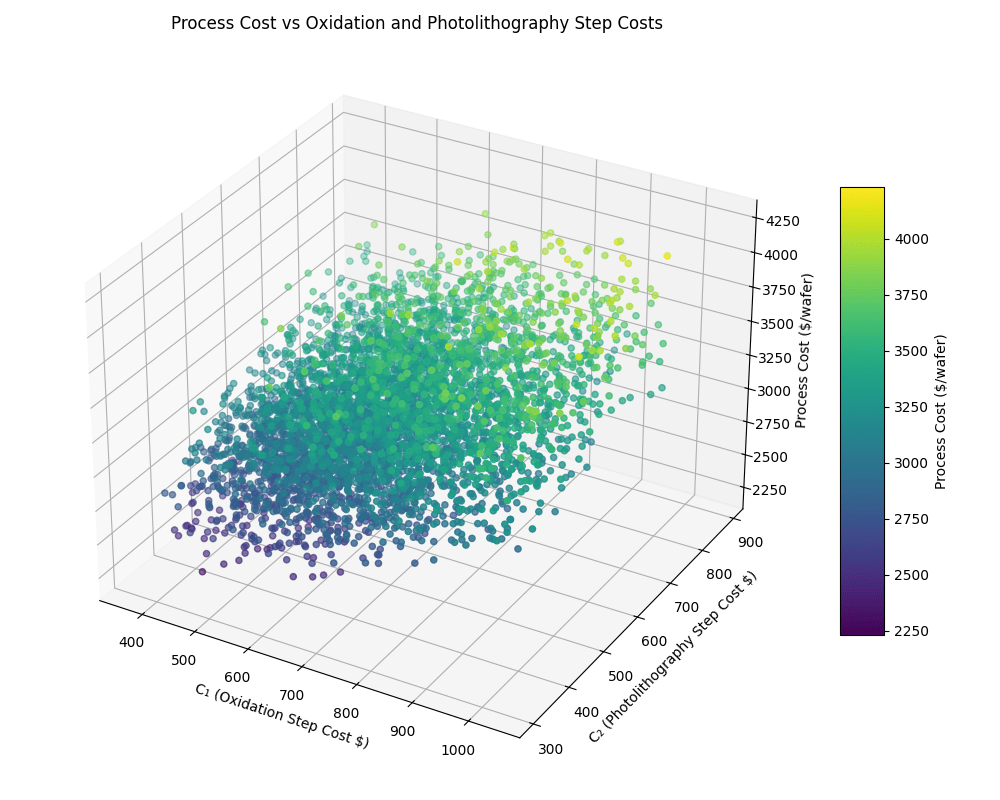
A 3D scatter plot of predicted process cost versus two representative step costs (Oxidation and Photolithography) is shown in Figure 3.
Figure 2. Process cost distribution as a function of oxidation (C₁) and photolithography (C₂) step costs. Each point corresponds to a single synthetic data sample.
This design represents a simple, generalizable Business ML framework that can be extended across other process-oriented domains. The neural network acts as a surrogate function that captures cost behavior across a space of operational inputs, without requiring manual calculations, spreadsheets, or symbolic optimization. The model was implemented using TensorFlow with the Keras API and trained on a MacBook M4 CPU without GPU acceleration. All experiments were performed in a lightweight, reproducible environment, using standard Python tools such as scikit-learn for scaling and evaluation.
Results and Evaluation
The trained model was evaluated on a holdout test set comprising 1000 samples (20% of the 5000 total synthetic records). These test samples were not seen during training and serve as an unbiased estimate of model performance.
The final model architecture, a 64-64-1 feedforward neural network trained with a batch size of 32, achieved the following results:
Test Set Performance
- R² (coefficient of determination): 0.8671
- Mean Absolute Error (MAE): $85.69
- Mean Squared Error (MSE): 10,371.34
These results indicate that the model explains approximately 87% of the variability in process cost and predicts values with an average absolute deviation of less than $86. Considering the total process cost ranged from approximately $2230 to $4230, this represents an error of roughly 2.7% — well within a range that is useful for decision support in production planning or cost forecasting.
Loss Curve Analysis
Training dynamics were monitored using validation loss, with early stopping applied to prevent overfitting. The model converged after 17 epochs, with validation loss reaching its minimum at epoch 7 and no further improvement thereafter. Early stopping restored the weights from this optimal point.
Figure 3. Training and validation loss curve during model training. Early stopping restored the best weights based on the lowest validation loss.
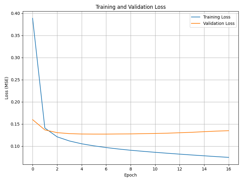
This convergence behavior confirms that the model was not overtrained and generalizes well to unseen data.
Scenario Testing
To test the model’s flexibility and real-world applicability, seven what-if scenarios were created by adjusting process step durations and cost rates. These included edge cases such as photolithography overload, implant bottlenecks, and optimized CMP/anneal conditions. The model returned consistent, interpretable cost predictions across all cases, demonstrating its ability to simulate the financial impact of changes in operational inputs.
The model outputs wafer-level process cost values that span a realistic operating range. Across 5000 synthetic samples with 5% noise, the predicted costs ranged from $2,229.98 to $4,230.61, with a mean of $3,181.06 and standard deviation of $285.75. This range serves as the reference context for interpreting the impact of scenario changes.
Figure 4 presents a comparison of seven scenarios designed to stress or improve different steps in the CMOS process. Each bar reflects the predicted process cost when modifying specific combinations of time and cost factors for one or more steps. These scenarios were evaluated using the trained neural network model.
Figure 4. Predicted process costs for seven scenario cases based on step-level time and cost modifications. The baseline reflects nominal midpoint values. Other scenarios simulate manufacturing disruptions (e.g., “Photolithography Crisis”) or optimizations (e.g., “Implant Optimization,” “Lean Operations”). Predictions were generated using the trained neural network model.
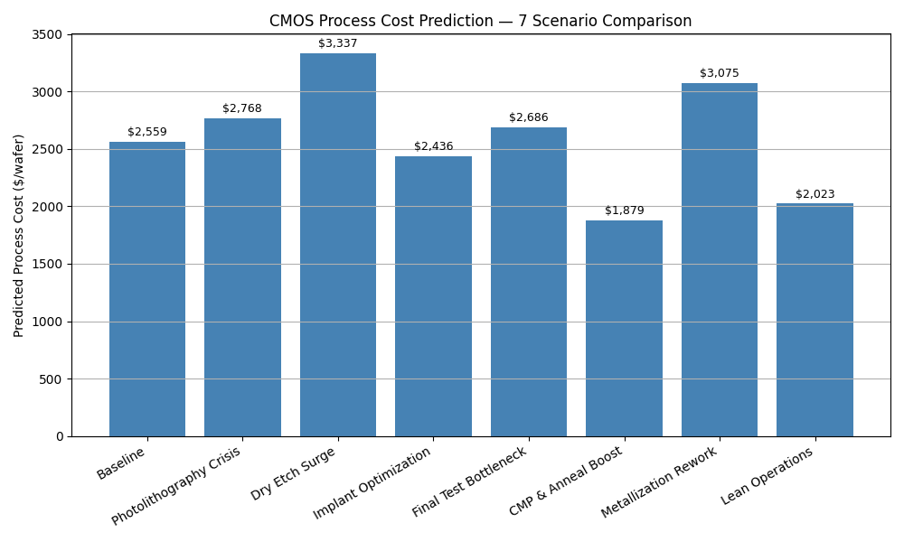
The baseline scenario uses the midpoint of each feature’s training range, scaled down to simulate a typical factory setting operating at 75% of nominal time and 85% of nominal cost. The baseline feature set is as follows:
- Baseline step durations (ti):
t0tot9: [9.38, 90.00, 26.25, 16.88, 11.25, 33.75, 22.50, 39.38, 33.75, 9.38] (minutes) - Baseline step costs (ci):
c0toc9: [3.83, 4.68, 13.60, 9.35, 11.90, 6.80, 5.95, 5.53, 8.10, 3.83] ($/minute)
All seven scenarios are derived by selectively modifying one or more of these values:
- Photolithography Crisis doubles both
t2andc2(photolithography duration and cost). - Dry Etch Surge increases
t3by 50% andc3by 150%. - Implant Optimization reduces both
t4andc4by 50%. - Final Test Bottleneck triples
t9and increasesc9by 50%. - CMP & Anneal Boost reduces
t6,c6,t7, andc7by 40%. - Metallization Rework doubles
t8and increasesc8by 20%. - Lean Operations reduces all
tivalues by 15% and allcivalues by 10%.
These cases were designed to test the model’s responsiveness to both localized disturbances and broad efficiency improvements. The predicted costs reflect the non-linear effects of compounding time and cost variations across multiple steps.
Conclusion
This study demonstrated how a simple feedforward neural network can be used to model the economics of CMOS wafer processing using structured time and cost inputs. By simulating realistic ranges for ten key fabrication steps and adding controlled noise to mimic real-world variability, the model was able to predict wafer processing cost with strong accuracy.
The final model, trained on just 5000 synthetic records with ±5% noise, achieved an R² of 0.8671 and an MAE of $85.69. These results reflect a high level of fidelity for a process whose total cost spans approximately $2000. The model also performed well across a range of simulated what-if scenarios, enabling economic forecasts for process changes without requiring manual recalculation or spreadsheet modeling.
More importantly, the CMOS case illustrates the broader value of Business ML. This approach generalizes to any structured process where cost accumulates over a series of steps, and where time and resource variability drive economic outcomes. Unlike static cost models, Business ML can learn from historical data and capture hidden variations in timing and resource usage that influence cost outcomes in subtle ways. These patterns, often invisible in spreadsheets, are preserved in operational data and can be exploited by ML models to deliver faster, more adaptive, and more insightful cost predictions. Business ML delivers both speed and precision, helping teams move from cost estimation to real-time cost intelligence.
Call to Action
Explore the Business ML demo and see cost prediction in action
The CMOS process cost prediction model featured in this article is now available as a live demonstration.
MLPowersAI develops custom machine learning models and deployment-ready solutions for structured, multistep manufacturing environments. This includes use cases in semiconductors, chemical production, and other industries where time, cost, and complexity converge. Our goal is to help teams harness their historical process data to forecast outcomes, optimize planning, and simulate business scenarios in real time.
In addition to semiconductor cost modeling, we apply similar Business ML frameworks across a wide range of process industries, including chemicals, pharmaceuticals, energy systems, food and beverage, and advanced materials — wherever domain data can be turned into faster, smarter economic decisions.
🔗 Visit us at MLPowersAI.com
🔗 Connect via LinkedIn for discussions or collaboration inquiries.
